stm32f4discovery 是很好的 os 練習平台, 不過沒有 mmu 是我覺得可惜的部份, 而 raspberrypi 2 正好可以補足這部份, 然而 rpi2 我目前還不知道怎麼使用 jtag, 在除錯上會比較麻煩, 得用冥想的。
沒想到第二個 bare-metal rpi2 程式就要搞 mmu 了, 感覺很硬斗, 我自己覺得還好, 畢竟我已經累積了不少
經驗/知識 。這就是累積的力量。
之前有寫過
x86 mmu 的文章, 那時候 mmu 並不是我重點學習的部份, 現在換個平台, 再來重新學習。
raspberrypi 2 是 arm cortex A7, 這是比較新的架構, 網路上找的 mmu 資訊大部份都是 arm v6 的, 而 DS-5 有 startup_Cortex-A7/startup.s 可以用來參考, 程式碼配合手冊, 可以加速學習速度。
我強烈建議你先看《
一步步写嵌入式操作系统:ARM编程的方法与实践 》3.2 ~ 3.4, 否則應該看不懂這篇, 除了理論 (在
一步步写嵌入式操作系统:ARM编程的方法与实践 說明的很詳細, 所以我不會說明 arm v6 mmu 工作方式, 這本書雖然絕版了卻很容易找到, 別擔心。這本書寫的雖是 arm v6, 但還是有很大的參考價值), 我還會展示實作的程式碼, 可以想成是
一步步写嵌入式操作系统:ARM编程的方法与实践 arm v7-A 真實機器 (rpi2) 的版本。
由於是 arm v7-A, 所以還要搭配 ARM®
Architecture Reference Manual ARMv7-A and ARMv7-R edition Chapter B3 Virtual Memory System Architecture (VMSA) 研讀 (因為我找不到中文的, 所以只好自己 K 英文手冊), 若你真的看過
一步步写嵌入式操作系统:ARM编程的方法与实践 , 再看這部份會好懂些。大同中有小異, cortex v7-A 多了一些欄位, 所以還是要參考一下手冊的內容。這部份有 200 多頁, 不過並不需要真的看完才會設定, 我大概看了 10 頁左右就足夠寫下這篇。
page 大小有以下四類, 我選用 sections, 這是 1MB 的大小, cortex v7-A 沒有 1K 大小的 page, 而且這只需要一個 page table, 不用出動到兩個 page table, 簡化我們的學習。
Supersections Consist of 16MB blocks of memory. Support for Supersections is optional, except that an implementation that includes the Large Physical Address Extension and supports more that 32 bits of Physical Address must also support Supersections to provide access to the entire Physical Address space.
Sections Consist of 1MB blocks of memory.
Large pages Consist of 64KB blocks of memory.
Small pages Consist of 4KB blocks of memory.
fig 2. virtual address 轉換為 physical address 的方式
fig 2 說明 virtual address 如何轉成 physical address, 在
一步步写嵌入式操作系统:ARM编程的方法与实践 p62, p63 有詳細的說明, 還提供了範例, 這個圖其實很直覺的, 前題是你得把那兩頁看完, 否則應該看不懂。
我要讓 physical address 0x3F000000 對應到 virtual address 0xc8000000, 應該怎麼填入 first-level descriptor, 也許你聽過 page table entry, 和 first-level descriptor 是一樣的東西, 這是 arm 手冊上的術語。
https://github.com/descent/arm_os/blob/master/leeos/chapter3/part2/cortex_a_mmu.c
這是我從
一步步写嵌入式操作系统:ARM编程的方法与实践 https://github.com/descent/arm_os/blob/master/leeos/chapter3/part2/mmu.c 改過來的, 可以先列印出 first-level descriptor 其存放位址與內容。
tt_ex 1 #define PHYSICAL_IO_ADDR 0x3F000000
2 #define VIRTUAL_IO_ADDR 0xc8000000
3 translation table base : 30700000
4
5 0 (IO) ## pte_addr: 30703200, pte: 3f000de2
6 1 (IO) ## pte_addr: 30703204, pte: 3f100de2
7 2 (IO) ## pte_addr: 30703208, pte: 3f200de2
translation table base register 是 30700000, 我們來看看一個 virtual address 0xc8000000 怎麼對應到 physical address 0x3F000000。注意哦! 第一筆 first-level descriptor 並不是在 30700000, 而是 30703200。
c80 00000 =>
c80 00000
c80 << 2 = 3200
30700000 | 3200 = 30703200
tt_ex L5就是我們要查找的 first-level descriptor, 其內容是 3f000de2。
3f0 00de2 橘色的
3f0 和
c80 00000 藍色的 00000 作 or 運算,
3f0 00000 就是最後的答案。
所以正確填好這個表, 就能正確轉換
實體/虛擬 位址, 你要怎麼轉就怎麼轉。不過實際上還要再複雜一點, 還有 ds-5/examples/DS-5Examples/startup_Cortex-A7/startup.s L218 ~ L232 的欄位要填, 請自己參閱手冊。
手冊相關章節
rpi2 有 1GB ram, arm address 從 0 開始, 所以 physical address 從 0x00000000 ~ 0x40000000, 我特別說明這個, 看起來好像是廢話, 其實不是這樣, 嵌入式系統的記憶體位址很有可能出乎你的想像, 有的 1GB 是從 0x10000000 開始算起的, 並不一定是從 0 算起, 每一家廠商的 soc 可能都不同。和書中一樣, ddr 的 mapping 我們用一對一, 也就是位址 0 經過 mmu 轉換後還是位址 0, 位址 99 經過 mmu 轉換後還是位址 99。
ds-5/examples/DS-5Examples/startup_Cortex-A7/startup.s 1 ;==================================================================
2 ; Copyright ARM Ltd 2005-2014. All rights reserved.
3 ;
4 ; Cortex-A7 Embedded example - Startup Code
5 ;==================================================================
6
7
8 ; Standard definitions of mode bits and interrupt (I & F) flags in PSRs
9
10 Mode_USR EQU 0x10
11 Mode_FIQ EQU 0x11
12 Mode_IRQ EQU 0x12
13 Mode_SVC EQU 0x13
14 Mode_ABT EQU 0x17
15 Mode_UND EQU 0x1B
16 Mode_SYS EQU 0x1F
17
18 I_Bit EQU 0x80 ; When I bit is set, IRQ is disabled
19 F_Bit EQU 0x40 ; When F bit is set, FIQ is disabled
20
21
22 PRESERVE8
23 AREA VECTORS, CODE, READONLY ; Name this block of code
24
25 ENTRY
26
27 ;==================================================================
28 ; Entry point for the Reset handler
29 ;==================================================================
30
31 EXPORT Start
32
33 Start
34
35 ;==================================================================
36 ; Exception Vector Table
37 ;==================================================================
38 ; Note: LDR PC instructions are used here, though branch (B) instructions
39 ; could also be used, unless the exception handlers are >32MB away.
40
41 Vectors
42 LDR PC, Reset_Addr
43 LDR PC, Undefined_Addr
44 LDR PC, SVC_Addr
45 LDR PC, Prefetch_Addr
46 LDR PC, Abort_Addr
47 LDR PC, Hypervisor_Addr
48 LDR PC, IRQ_Addr
49 LDR PC, FIQ_Addr
50
51 Reset_Addr DCD Reset_Handler
52 Undefined_Addr DCD Undefined_Handler
53 SVC_Addr DCD SVC_Handler
54 Prefetch_Addr DCD Prefetch_Handler
55 Abort_Addr DCD Abort_Handler
56 Hypervisor_Addr DCD Hypervisor_Handler
57 IRQ_Addr DCD IRQ_Handler
58 FIQ_Addr DCD FIQ_Handler
59
60
61 ;==================================================================
62 ; Exception Handlers
63 ;==================================================================
64
65 Undefined_Handler
66 B Undefined_Handler
67 SVC_Handler
68 B SVC_Handler
69 Prefetch_Handler
70 B Prefetch_Handler
71 Abort_Handler
72 B Abort_Handler
73 Hypervisor_Handler
74 B Hypervisor_Handler
75 IRQ_Handler
76 B IRQ_Handler
77 FIQ_Handler
78 B FIQ_Handler
79
80
81 ;==================================================================
82 ; Reset Handler
83 ;==================================================================
84 Reset_Handler FUNCTION {}
85
86 ;==================================================================
87 ; Disable caches, MMU and branch prediction in case they were left enabled from an earlier run
88 ; This does not need to be done from a cold reset
89 ;==================================================================
90
91 MRC p15, 0, r0, c1, c0, 0 ; Read CP15 System Control register
92 BIC r0, r0, #(0x1 << 12) ; Clear I bit 12 to disable I Cache
93 BIC r0, r0, #(0x1 << 2) ; Clear C bit 2 to disable D Cache
94 BIC r0, r0, #0x1 ; Clear M bit 0 to disable MMU
95 BIC r0, r0, #(0x1 << 11) ; Clear Z bit 11 to disable branch prediction
96 MCR p15, 0, r0, c1, c0, 0 ; Write value back to CP15 System Control register
97
98 ; The MMU is enabled later, before calling main(). Caches and branch prediction are enabled inside main(),
99 ; after the MMU has been enabled and scatterloading has been performed.
100
101 ;===================================================================
102 ; ACTLR.SMP Enables coherent requests to the processor.
103 ; You must ensure this bit is set to 1 before the caches and MMU are enabled, or any cache and TLB maintenance operations are performed.
104 ;===================================================================
105 MRC p15, 0, r0, c1, c0, 1 ; Read CP15 ACTLR
106 ORR r0, r0, #(1 << 6) ; set ACTLR.SMP bit
107 MCR p15, 0, r0, c1, c0, 1 ; Write CP15 ACTLR
108
109 ;==================================================================
110 ; Invalidate Data and Instruction TLBs and branch predictor in case they were left enabled from an earlier run
111 ; This does not need to be done from a cold reset
112 ;==================================================================
113
114 MOV r0,#0
115 MCR p15, 0, r0, c8, c7, 0 ; I-TLB and D-TLB invalidation
116 MCR p15, 0, r0, c7, c5, 6 ; BPIALL - Invalidate entire branch predictor array
117
118 ;==================================================================
119 ; Initialize Supervisor Mode Stack
120 ; Note stack must be 8 byte aligned.
121 ;==================================================================
122
123 IMPORT ||Image$$ARM_LIB_STACK$$ZI$$Limit|| ; Linker symbol from scatter file
124 LDR SP, =||Image$$ARM_LIB_STACK$$ZI$$Limit||
125
126 ;===================================================================
127 ; Set Vector Base Address Register (VBAR) to point to this application's vector table
128 ;===================================================================
129
130 LDR r0, =Vectors
131 MCR p15, 0, r0, c12, c0, 0
132
133 ;==================================================================
134 ; Cache Invalidation code for Cortex-A7
135 ; NOTE: Neither Caches, nor MMU, nor BTB need post-reset invalidation on Cortex-A7,
136 ; but forcing a cache invalidation, makes the code more portable to other CPUs (e.g. Cortex-A9)
137 ;==================================================================
138 ; Invalidate L1 Instruction Cache
139 MRC p15, 1, r0, c0, c0, 1 ; Read Cache Level ID Register (CLIDR)
140 TST r0, #0x3 ; Harvard Cache?
141 MOV r0, #0 ; SBZ
142 MCRNE p15, 0, r0, c7, c5, 0 ; ICIALLU - Invalidate instruction cache and flush branch target cache
143
144 ; Invalidate Data/Unified Caches
145
146 MRC p15, 1, r0, c0, c0, 1 ; Read CLIDR
147 ANDS r3, r0, #0x07000000 ; Extract coherency level
148 MOV r3, r3, LSR #23 ; Total cache levels << 1
149 BEQ Finished ; If 0, no need to clean
150
151 MOV r10, #0 ; R10 holds current cache level << 1
152 Loop1 ADD r2, r10, r10, LSR #1 ; R2 holds cache "Set" position
153 MOV r1, r0, LSR r2 ; Bottom 3 bits are the Cache-type for this level
154 AND r1, r1, #7 ; Isolate those lower 3 bits
155 CMP r1, #2
156 BLT Skip ; No cache or only instruction cache at this level
157
158 MCR p15, 2, r10, c0, c0, 0 ; Write the Cache Size selection register
159 ISB ; ISB to sync the change to the CacheSizeID reg
160 MRC p15, 1, r1, c0, c0, 0 ; Reads current Cache Size ID register
161 AND r2, r1, #7 ; Extract the line length field
162 ADD r2, r2, #4 ; Add 4 for the line length offset (log2 16 bytes)
163 LDR r4, =0x3FF
164 ANDS r4, r4, r1, LSR #3 ; R4 is the max number on the way size (right aligned)
165 CLZ r5, r4 ; R5 is the bit position of the way size increment
166 LDR r7, =0x7FFF
167 ANDS r7, r7, r1, LSR #13 ; R7 is the max number of the index size (right aligned)
168
169 Loop2 MOV r9, r4 ; R9 working copy of the max way size (right aligned)
170
171 Loop3 ORR r11, r10, r9, LSL r5 ; Factor in the Way number and cache number into R11
172 ORR r11, r11, r7, LSL r2 ; Factor in the Set number
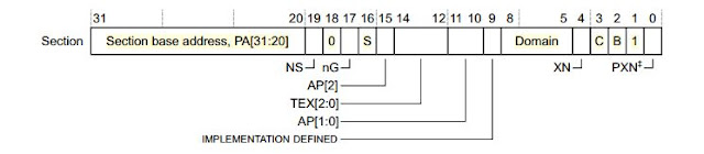
173 MCR p15, 0, r11, c7, c6, 2 ; Invalidate by Set/Way
174 SUBS r9, r9, #1 ; Decrement the Way number
175 BGE Loop3
176 SUBS r7, r7, #1 ; Decrement the Set number
177 BGE Loop2
178 Skip ADD r10, r10, #2 ; increment the cache number
179 CMP r3, r10
180 BGT Loop1
181
182 Finished
183
184
185 ;===================================================================
186 ; Cortex-A7 MMU Configuration
187 ; Set translation table base
188 ;===================================================================
189
190 IMPORT ||Image$$VECTORS$$Base|| ; From scatter file
191 IMPORT ||Image$$TTB$$ZI$$Base|| ; From scatter file
192
193 ; Cortex-A7 supports two translation tables
194 ; Configure translation table base (TTB) control register cp15,c2
195 ; to a value of all zeros, indicates we are using TTB register 0.
196
197 MOV r0,#0x0
198 MCR p15, 0, r0, c2, c0, 2
199
200 ; write the address of our page table base to TTB register 0
201 LDR r0,=||Image$$TTB$$ZI$$Base||
202 MOV r1, #0x08 ; RGN=b01 (outer cacheable write-back cached, write allocate)
203 ; S=0 (translation table walk to non-shared memory)
204 ORR r1,r1,#0x40 ; IRGN=b01 (inner cacheability for the translation table walk is Write-back Write-allocate)
205
206 ORR r0,r0,r1
207 MCR p15, 0, r0, c2, c0, 0 208
209
210 ;===================================================================
211 ; PAGE TABLE generation
212
213 ; Generate the page tables
214 ; Build a flat translation table for the whole address space.
215 ; ie: Create 4096 1MB sections from 0x000xxxxx to 0xFFFxxxxx
216
217
218 ; 31 20 19 18 17 16 15 14 12 11 10 9 8 5 4 3 2 1 0
219 ; |section base address| 0 0 |nG| S |AP2| TEX | AP | P | Domain | XN | C B | 1 0|
220 ;
221 ; Bits[31:20] - Top 12 bits of VA is pointer into table
222 ; nG[17]=0 - Non global, enables matching against ASID in the TLB when set.
223 ; S[16]=0 - Indicates normal memory is shared when set.
224 ; AP2[15]=0
225 ; AP[11:10]=11 - Configure for full read/write access in all modes
226 ; TEX[14:12]=000
227 ; CB[3:2]= 00 - Set attributes to Strongly-ordered memory.
228 ; (except for the code segment descriptor, see below)
229 ; IMPP[9]=0 - Ignored
230 ; Domain[5:8]=1111 - Set all pages to use domain 15
231 ; XN[4]=1 - Execute never on Strongly-ordered memory
232 ; Bits[1:0]=10 - Indicate entry is a 1MB section233 ;===================================================================
234 LDR r0,=||Image$$TTB$$ZI$$Base||
235 LDR r1,=0xfff ; loop counter
236 LDR r2,=2_00000000000000000000110111100010
237
238 ; r0 contains the address of the translation table base
239 ; r1 is loop counter
240 ; r2 is level1 descriptor (bits 19:0)
241
242 ; use loop counter to create 4096 individual table entries.
243 ; this writes from address 'Image$$TTB$$ZI$$Base' +
244 ; offset 0x3FFC down to offset 0x0 in word steps (4 bytes)
245
246 init_ttb_1
247 ORR r3, r2, r1, LSL#20 ; R3 now contains full level1 descriptor to write
248 ORR r3, r3, #2_0000000010000 ; Set XN bit
249 STR r3, [r0, r1, LSL#2] ; Str table entry at TTB base + loopcount*4
250 SUBS r1, r1, #1 ; Decrement loop counter
251 BPL init_ttb_1
252
253 ; In this example, the 1MB section based at '||Image$$VECTORS$$Base||' is setup specially as cacheable (write back mode).
254 ; TEX[14:12]=001 and CB[3:2]= 11, Outer and inner write back, write allocate normal memory.
255 LDR r1,=||Image$$VECTORS$$Base|| ; Base physical address of code segment
256 LSR r1, #20 ; Shift right to align to 1MB boundaries
257 ORR r3, r2, r1, LSL#20 ; Setup the initial level1 descriptor again
258 ORR r3, r3, #2_0000000001100 ; Set CB bits
259 ORR r3, r3, #2_1000000000000 ; Set TEX bit 12
260 STR r3, [r0, r1, LSL#2] ; str table entry
261
262 ;===================================================================
263 ; Setup domain control register - Enable all domains to client mode
264 ;===================================================================
265
266 MRC p15, 0, r0, c3, c0, 0 ; Read Domain Access Control Register
267 LDR r0, =0x55555555 ; Initialize every domain entry to b01 (client)
268 MCR p15, 0, r0, c3, c0, 0 ; Write Domain Access Control Register
269
270 IF {TARGET_FEATURE_NEON} || {TARGET_FPU_VFP}
271 ;==================================================================
272 ; Enable access to NEON/VFP by enabling access to Coprocessors 10 and 11.
273 ; Enables Full Access i.e. in both privileged and non privileged modes
274 ;==================================================================
275
276 MRC p15, 0, r0, c1, c0, 2 ; Read Coprocessor Access Control Register (CPACR)
277 ORR r0, r0, #(0xF << 20) ; Enable access to CP 10 & 11
278 MCR p15, 0, r0, c1, c0, 2 ; Write Coprocessor Access Control Register (CPACR)
279 ISB
280
281 ;==================================================================
282 ; Switch on the VFP and NEON hardware
283 ;=================================================================
284
285 MOV r0, #0x40000000
286 VMSR FPEXC, r0 ; Write FPEXC register, EN bit set
287 ENDIF
288
289
290 ;===================================================================
291 ; Enable MMU and branch to __main
292 ; Leaving the caches disabled until after scatter loading.
293 ;===================================================================
294
295 IMPORT __main ; Before MMU enabled import label to __main
296
297 LDR r12,=__main ; Save this in register for possible long jump
298
299 MRC p15, 0, r0, c1, c0, 0 ; Read CP15 System Control register
300 BIC r0, r0, #(0x1 << 12) ; Clear I bit 12 to disable I Cache
301 BIC r0, r0, #(0x1 << 2) ; Clear C bit 2 to disable D Cache
302 BIC r0, r0, #0x2 ; Clear A bit 1 to disable strict alignment fault checking
303 ORR r0, r0, #0x1 ; Set M bit 0 to enable MMU before scatter loading
304 MCR p15, 0, r0, c1, c0, 0 ; Write CP15 System Control register
305
306 ; Now the MMU is enabled, virtual to physical address translations will occur. This will affect the next
307 ; instruction fetch.
308 ;
309 ; The two instructions currently in the ARM pipeline will have been fetched before the MMU was enabled.
310 ; The branch to __main is safe because the Virtual Address (VA) is the same as the Physical Address (PA)
311 ; (flat mapping) of this code that enables the MMU and performs the branch
312
313 BX r12 ; Branch to __main C library entry point
314
315 ENDFUNC
316
317
318
319 ;==================================================================
320 ; Enable caches and branch prediction
321 ; This code must be run from a privileged mode
322 ;==================================================================
323
324 AREA ENABLECACHES, CODE, READONLY
325
326 EXPORT enable_caches
327
328 enable_caches FUNCTION
329
330 ;==================================================================
331 ; Enable caches and branch prediction
332 ;==================================================================
333
334 MRC p15, 0, r0, c1, c0, 0 ; Read System Control Register
335 ORR r0, r0, #(0x1 << 12) ; Set I bit 12 to enable I Cache
336 ORR r0, r0, #(0x1 << 2) ; Set C bit 2 to enable D Cache
337 ORR r0, r0, #(0x1 << 11) ; Set Z bit 11 to enable branch prediction
338 MCR p15, 0, r0, c1, c0, 0 ; Write System Control Register
339
340 BX lr
341
342 ENDFUNC
343
344
345 END
https://github.com/descent/arm_os/blob/master/leeos/chapter3/part2/cortex_a_mmu.c 是我參考了 ds-5/examples/DS-5Examples/startup_Cortex-A7/startup.s 其他屬性設定最後的結果, 和 ds-5/examples/DS-5Examples/startup_Cortex-A7/startup.s 有些不同, 請自己參考並配合手冊說明來讀懂它們, 你願意看這篇文章, 我相信手冊的內容應該難不倒你。
和書中以模擬器執行程式不同, 真實機器上可有很多細節要處理, 還好有人做好這些事情了。我的測試方式從 uart 開始, uart05.c 是 uart 的程式碼, 可以透過 uart 顯示字元到 minicom 上, 從
https://github.com/dwelch67/raspberrypi fork 來的, 我仿照書中的想法, 將這程式修改加入 mmu 之後, 再從轉換的位址印出字元。
uart05.c L64, L77 0x3f215040 就是 uart 送出字元的暫存器實體位址, 0xc8215040 則是用 mmu 轉換過後的虛擬位址, 所以在啟動 mmu 後, 就要寫入 0xc8215040 這位址才能正確在 uart 上送出字元。
uart 轉換 first-level descriptor 0 (IO) ## pte_addr: 30703200, pte: 3f000de2
1 (IO) ## pte_addr: 30703204, pte: 3f100de2
2 (IO) ## pte_addr: 30703208, pte: 3f200de2
大家可以算算看, 0xc8215040 是不是會對應到 0x3f215040。
uart05.c 1
2 //-------------------------------------------------------------------------
3 //-------------------------------------------------------------------------
4
5 // 2 outer corner
6 // 4
7 // 6
8 // 8 TX out
9 // 10 RX in
10
11 extern void PUT32 ( unsigned int, unsigned int );
12 extern void PUT16 ( unsigned int, unsigned int );
13 extern void PUT8 ( unsigned int, unsigned int );
14 extern unsigned int GET32 ( unsigned int );
15 extern unsigned int GETPC ( void );
16 extern void dummy ( unsigned int );
17 extern unsigned int BRANCHTO ( unsigned int );
18
19 extern void uart_init ( void );
20 extern unsigned int uart_lcr ( void );
21 extern void uart_flush ( void );
22 extern void uart_send ( unsigned int );
23 extern unsigned int uart_recv ( void );
24 extern unsigned int uart_check ( void );
25 extern void hexstring ( unsigned int );
26 extern void hexstrings ( unsigned int );
27 extern void timer_init ( void );
28 extern unsigned int timer_tick ( void );
29
30 extern void timer_init ( void );
31 extern unsigned int timer_tick ( void );
32
33 //------------------------------------------------------------------------
34 int notmain ( void )
35 {
36 // form : arm_os/leeos/chapter3/part2/cortex_a_mmu.c
37 void init_sys_mmu(void);
38 void start_mmu(void);
39
40 uart_init();
41
42 uart_send(0x0D);
43 uart_send(0x0A);
44
45 // uart_send
46
47 while(1)
48 {
49 if (*(volatile unsigned int *)(0x3F000000 + 0x00215054) & 0x20) break;
50 }
51 *(volatile unsigned int *)(0x3F000000 + 0x00215040) = 0x31;
52
53 while(1)
54 {
55 if (*(volatile unsigned int *)(0x3F000000 + 0x00215054) & 0x20) break;
56 }
57 *(volatile unsigned int *)(0x3F000000 + 0x00215040) = 0x32;
58
59 while(1)
60 {
61 //if(GET32(AUX_MU_LSR_REG)&0x20) break;
62 if (*(volatile unsigned int *)(0x3F000000 + 0x00215054) & 0x20) break;
63 }
64 *(volatile unsigned int *)(0x3F000000 + 0x00215040) = 0x33;65
66 uart_send(0x0D);
67 uart_send(0x0A);
68
69 init_sys_mmu();
70 start_mmu();
71
72 while(1)
73 {
74 //if(GET32(AUX_MU_LSR_REG)&0x20) break;
75 if (*(volatile unsigned int *)(0xc8000000 + 0x00215054) & 0x20) break;
76 }
77 *(volatile unsigned int *)(0xc8000000 + 0x00215040) = 'A';78
79 while(1)
80 {
81 //if(GET32(AUX_MU_LSR_REG)&0x20) break;
82 if (*(volatile unsigned int *)(0xc8000000 + 0x00215054) & 0x20) break;
83 }
84 *(volatile unsigned int *)(0xc8000000 + 0x00215040) = 'B';
85
86 while(1)
87 {
88 //if(GET32(AUX_MU_LSR_REG)&0x20) break;
89 if (*(volatile unsigned int *)(0xc8000000 + 0x00215054) & 0x20) break;
90 }
91 *(volatile unsigned int *)(0xc8000000 + 0x00215040) = 'C';
92
93 while(1);
94
95 return(0);
96 }
設定 mmu 有幾點前提:
translation table base 要設在哪個位址, 這是 page table 的 base address, 我是設定在 0x30700000。
實體記憶的位址要對應到哪個虛擬位址。
page 權限設定。
我沒想過有那麼好的運氣, 一次就成功, 看看以下的結果, 只有輸出 123ABC, 是不是很單調, 不過可別小看這個印出的結果, 你我都知道, 這可是得來不易。
你得克服:
硬體的 uart 接線
開機程式的撰寫
uart 程式可以正常運作
mmu 的相關設定
最後才能得到這個印到 minicom 的結果, 每一步都不是容易的一件事。若你保持毅力跟到這裡, 給自己拍拍手, 你一定像我一樣, 打算往底層知識繼續挖掘下去, 加油, 這和娃坑一樣, 是個無底洞。請保持享受苦澀後的甘甜般的決心, 「知道」後的開心便是我能如此繼續下去的動力。
123 是在 mmu 起動之前印出, ABC 是經過 mmu 位址轉換後印出。
test result (minicom setting 115200 8N1) Welcome to minicom 2.6.2
OPTIONS: I18n
Compiled on Feb 7 2013, 21:36:21.
Port /dev/ttyUSB0, 10:22:43
Press CTRL-A Z for help on special keys
123
ABC
現在你知道 mmu 轉換位址的魔法了, 她沒在那麼神祕了。
source code 有兩部份:
得把 cortex_a_mmu.c 複製到 uart_mmu 目錄下, 才能正確在 uart_mmu 產生出執行檔, 很麻煩我知道, 不過我想不到好辦法。
做出很多人用的手機 app 很有趣。
做出很有創意的網路服務也令人佩服。
了解底層的祕密也很令人開心。
ref:
沒有留言:
張貼留言
使用 google 的 reCAPTCHA 驗證碼, 總算可以輕鬆留言了。
我實在受不了 spam 了, 又不想讓大家的眼睛花掉, 只好放棄匿名留言。這是沒辦法中的辦法了。留言的朋友需要有 google 帳號。